

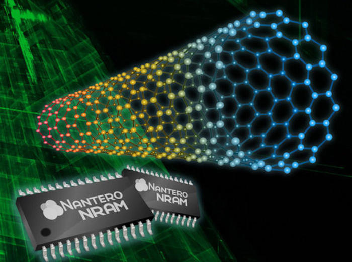
Carbon nanotubes that are not in contact with each other are in the high resistance state that represents the ‘off” or ‘0’ state. When the carbon nanotube contact each other, they take on the low-resistance state of ‘on’ or ‘1’.
“The combination of Nantero’s technology with our design and production capabilities promises to meet the longstanding needs of our customers for non-volatile memory that is higher density, faster, more energy efficient and with a higher rewrite cycle,” Masato Matsumiya, vice president of Fujitsu Semiconductor, said in a statement.
Denser memory
NRAM has the potential to create memory that is vastly denser than NAND Flash, which is used today in thumb drives and solid state drives. The densest NAND Flash process today is near 15 nanometres, which refers to the size of the transistors used to store bits of data. NRAM can reach densities of below 5 nanometres, according to Schmergel.
Fujitsu plans to initially manufacture the NRAM using a 55-nanometer (nm) process. At that size, the initial memory modules will only be able to store megabytes of data. However, the company also plans a next-generation 40nm-process NRAM version, Schmergel said.
(In 2015, seven fabrication plants began limited manufacturing of the superfast carbon nanotube memory.)
Another big advantage NRAM has over traditional NAND Flash is its resistance to heat. It can withstand up to 300 degrees Celsius. Nantero claims its memory can last thousands of years at 85 degrees Celsius and has been tested at 300 degrees Celsius for 10 years. Not one bit of data was lost.
Venture capital
In December, Nantero received an additional $21 million (€19.7 million) in venture funding, bringing its total to $110 million (€103 million), “solidifying our hunch that this technology is about to break into the open,” Fitzgerald said in the report.
Unlike recent announcements by Intel and development partner Micron of their 3D XPoint non-volatile memory, which uses the PCIe/NVMe motherboard interface, NRAM uses DDR4 DRAM interface.
Spivey said he was somewhat surprised that Nantero’s memory will initially keep the DRAM interface.
“It seems to me a bit timid. That means there will be combinations of different types of memory used for quite a while, and certainly that is Fujitsu’s direct intention,” Spivey stated in an e-mail reply to Computerworld.
Even so, BCC Research expects NRAM to quickly affect consumer electronics, mobile computing, the Internet of Things, enterprise storage, defense, aeronautics and automotive. Others agree.
“This is one of very few technologies that’s moved beyond the research lab into high-volume manufacturing CMOS facilities,” Gregory Wong, an analyst with Forward Insights said in an earlier statement. “NRAM’s unique combination of high speed and high endurance has the potential to enable innovative products in a host of consumer and enterprise applications.”
IDG News Service


Subscribers 0
Fans 0
Followers 0
Followers