

As questions persist about the longevity of Moore’s Law, an analyst has predicted some specific ways that Intel will keep it going for at least the next few years.
Intel can continue to pack smaller transistors on its chips by using exotic materials and a new transistor design described by David Kanter, an analyst at Linley Group, in an article he published.
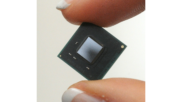
Intel currently manufactures chips using a 14-nanometer process, and is preparing its move to 10-nm later this year or early next. The number refers approximately to the smallest circuit dimensions etched on each chip, and smaller circuits mean faster chips and less power use.
7nm process
The new techniques could allow Intel to ensure the continuation of Moore’s Law, which recently turned 50, until at least the 7nm process, which Kanter estimates will come into production in 2017 or 2018.
Moore’s Law predicts that transistor density will double approximately every two years, allowing chips to get progressively faster and cheaper. But with transistors reaching atomic scale, electricity leakage and power management become more challenging.
Intel has introduced technologies such as strained silicon, high-k metal gate and FinFET, in which transistors are built upward in a 3D fashion instead of lying flat, to keep Moore’s Law going.
In the coming years, Kanter predicts it will combine silicon with materials such as strained germanium, or indium-gallium-arsenide, which part of a family III-V materials based on elements from the third and fifth columns of the periodic table.
Silicon successors
The III-V materials are being considered as eventual successors to silicon because they are better conductors of electrons. Initially, the materials are expected to be used alongside silicon. Intel is already using silicon alternatives like hafnium in its chips.
Also likely for future chips is a new transistor and gate structure based on quantum-well FETs (QWFETs), which Intel has been researching for a little under a decade. Here, electrons are sandwiched between III-V materials and gates on each side, ensuring the electrons move in the right direction. The behaviour of the charge becomes tightly controlled by the combination of the geometry and materials, and as a result transistors perform better.
Feasibility
Intel declined to comment on Kanter’s study. But the company has talked about the viability of QWFETs and III-V materials, and the feasibility of building chips based on the new transistor structure.
Kanter said that the new technologies are the best options available for cramming still more transistors onto chips.
Other required technologies, such as extreme ultraviolet (EUV) lithography, are not yet available from tool makers. Intel has instead taken to techniques like triple-patterning to make sure it can create chips with fewer defects. It ran into trouble with its 14-nm process, which led to a delay in the shipment of chips for PC, mobile and servers.
Kanter said he published his predictions in part because he feels it is the job of industry analysts to make specific, insightful forecasts, rather than vague guesses. “Simply saying that a new process technology will be better is vacuous,” he said.
“In reality, it will take months or years for Intel and the rest of the industry to reveal their plans for 10nm and 7nm,” he wrote. “In the meantime, this informed speculation should lead to some interesting discussions.”
Agam Shah, IDG News Service


Subscribers 0
Fans 0
Followers 0
Followers