

Intel reveals more of Tremont Atom core powering Surface Neo, Lakefield chip
Intel has formally unveiled Tremont, its next-generation Atom processor core and one half of the processor duo that will make up Lakefield and power Microsoft’s upcoming Surface Neo.
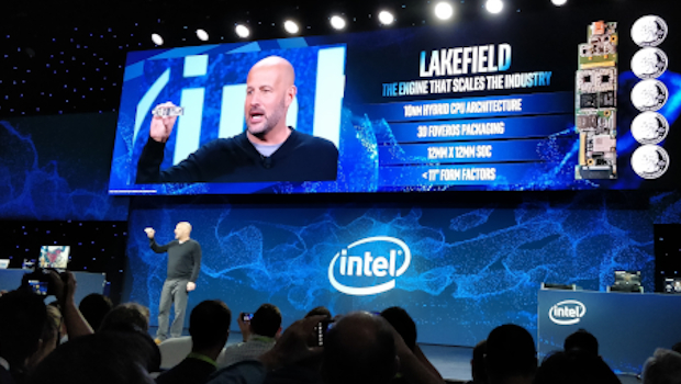
The company is describing the Tremont design in detail at the Linley Fall Processor Conference. Intel disclosed Tremont as early as this past January’s CES showcase, when it introduced Lakefield, a novel hybrid architecture with both the Tremont and Core processors working together. It is fair to say that this is a case of a mystery wrapped in an enigma, as the only announced product using Lakefield is Microsoft’s Surface Neo, a dual-screen PC-like device due in 2020, that Microsoft showed briefly a few weeks ago.
With Tremont, at least, we can start teasing out more of the mysteries underlying the Surface Neo and Lakefield. Because Tremont is a processor architecture, like the Sunny Cove architecture underlying Intel’s 10th-generation Ice Lake Core chips, certain specifics—such as clock speed, say—must wait until actual products hit the market. But we know the roles being assigned to Tremont: According to Stephen Robinson, a senior principal engineer at Intel, Tremont is being designed for networking, PC, and IoT devices.

Products built around Tremont will consume between 0.5W to 2W. Lakefield, and the Tremont cores within it, are being fabricated using Intel’s 10nm process. Single-threaded performance will be a substantial 30 percent higher than its predecessor, Goldmont Plus, based upon the SPECint and SPECfp benchmarks, Intel says.

Low power, but not underpowered
In Lakefield, Tremont is considered the “little” core, a term pioneered by ARM’s “big-little” architecture. CPU-intensive tasks are handled by powerful mainstream cores, while background tasks are handled by power-sipping “little” cores to keep overall power down. Sunny Cove-based cores handle the heavy lifting within Lakefield. Though many assumed Tremont would be underpowered as a consequence, Robinson said that is not true.

“That’s actually one of our beliefs when it comes to hybrid computing,” Robinson said. “You don’t want a very underperforming core to be in that hybrid solution. No one wants to be sad when their [instruction] thread gets saddled on that little core.”
Tremont is the successor to the Atom architecture known as Goldmont Plus, which later became the Gemini Lake desktop and mobile PC cores. Chances are that you never encountered Gemini Lake unless you bought a cheap desktop or notebook PC: The 1.5 GHz J5005, a Pentium Silver processor, was built around the Goldmont Plus architecture, as was the N5000. The latter powered devices like the sub-$300 (€270) Acer Swift 1, the HP 15-da0000, and others.
That is a long way of saying that in addition to Lakefield and the Surface Neo, you will see Tremont in familiar devices, including low-end laptops and NUCs, Robinson said. “This core is capable of satisfying those markets,” he added.
Robinson added that Tremont is being optimised for single-threaded performance, which typically means most general-purpose applications. In Lakefield, Tremont will be assigned background tasks, Intel has said.

The nuts and bolts
Five years ago, Atom devices might not have been all that interesting. Tremont’s role as the “little” core along with the “big” core in Lakefield, however, opens a new front in computing whose impact remains to be seen. The following details are mainly of interest to chip designers and device makers, who may or may not be building devices around Tremont.
Like the Goldmont Plus architecture, Tremont is being designed around a quad-core module, with each core sharing a single unified pool of between 1.5MB and 4.5MB of level-2 cache, depending upon the product. (That is a little unusual, as processor cores usually have their own dedicated Level 2 cache.) Because Tremont also supports Intel fabrics, Intel could even build in a Level 3 cache, either inclusive or non-inclusive, for additional performance, Robinson said.

Instructions are fetched using what Robinson called “Core-class” branch prediction, then decoded using a pair of three-wide clusters that use out-of-order decode. Put another way, if a nine-instruction loop is executed across one cluster, requiring three cycles to complete, Tremont can send the next iteration of the loop to the other cluster for processing, if it is predicted early enough, Robinson said. It essentially provides instructions more efficiently to a wider back end, Intel, says, which is important for performance. Tremont also forgoes the use of a micro-operations cache for this task.
Tremont includes dual 128-bit AES units for cryptographic acceleration, single instruction (4 cycle) SHA256, and Galois Field new instructions. Security protections such as trusted boot and Intel’s Total Memory Encryption have been designed in, as well as Intel’s Speed Shift, which uses hardware to quickly dial up and down clock speed.
All of these details are mainly of interest to chip designers and device makers, who may or may not be building devices around Tremont, anyway. Lakefield, however, is interesting, as are the devices that will be potentially built around it. Knowing a bit more about one of the CPU cores inside it tells us more about what those devices are capable of.
IDG News Service


Subscribers 0
Fans 0
Followers 0
Followers