

Toshiba has announced the development of the first 48-layer, three-dimensional Flash memory. Based on a vertical stacking technology that Toshiba calls Bit Cost Scaling (BiCS), the new flash memory stores two bits of data per transistor, meaning it is a multi-level cell (MLC) flash chip. It can store 128Gbits (16Gb) per chip. Sample shipments of products using the new process technology have already began.
Toshiba first announced its efforts to create 3D NAND flash chips in a partnership agreement with SanDisk last year.
Also last year, Samsung became the first company to announce it was mass-producing 3D flash chips, which it calls V-NAND. Those chips stacked 32-layers of transistors. Samsung’s V-NAND however, crams in 3-bits per transistor in what the industry refers to as triple-level cell (TLC) NAND. Because Samsung uses TLC memory, its chips are also able to store as much as Toshiba’s 48-layer 3D NAND – 128Gbits or 16Gb.
In a separate announcement, Intel and Micron said they would also begin producing 32-layer 3D NAND.
With the 3D NAND chips, which have started shipping, solid-state drives (SSDs) with more than 10Tb of storage are just around the corner, according to Brian Shirley, vice president of memory and technology solutions at Micron.
The new 3D Flash chips could be used to make M.2 expansion cards with more than 3.5TB of capacity for high-end tablets and ultralight laptops. In smart phones, the NAND flash will enable two to three times the 128Gb top capacities of current planar (2D) NAND, while not increasing costs.
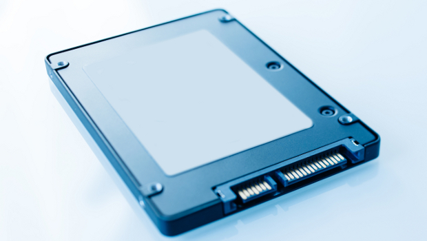
Toshiba said its 48-layer stacking process enhances the reliability of write/erase endurance, boosts write speed, and is suited for use in diverse applications, primarily solid-state drives (SSD).
Using a 48-layer NAND Flash allows Toshiba to revert to larger NAND process technologies. The company had scaled its 2D NAND down to 15 nanometers (nm), but it was bumping up against a wall in terms of further size reduction because as NAND transistor size shrinks, electrons tend to leak, causing data errors.
With 3D NAND, Toshiba will again be using larger 30nm, 40nm and even 50nm lithography to create NAND Flash, according to Scott Nelson, senior vice president of Toshiba’s memory business division.
Along with reliability and performance increases, the other benefit of 3D NAND for Toshiba will be cost reduction – the more dense the memory, the less silicon it needed to produce it. Once mass production begins in the second quarter of next year, however, prices for consumers of the technology will also begin to drop, Nelson said.
Eventually, Toshiba will begin to shrink the lithography process, enabling it to also offer the industry significantly higher capacity SSDs, Nelson said.
“The announcement today involves MLC, but we’ll be talking in the future about TLC for our 3D NAND,” he said.
The company is readying for mass production in the new Fab2 at Yokkaichi Operations in Japan. Fab2 is now under construction and will be completed in the first half of 2016, to meet growing demand for flash memory.
Lucas Mearian, IDG News Service


Subscribers 0
Fans 0
Followers 0
Followers