

One of the hottest topics in robotics is self-assembly, and any technique that requires no human intervention is of special interest.
The technology is also highly desirable for chips. Computing devices are shrinking thanks to smaller chips, which are reaching their physical limits.
Researchers from the Massachusetts Institute of Technology (MIT) and the University of Chicago have come up with a unique technique for self-assembling that could be used to cram more features onto small chip geometries.
The technology is one way to continue Moore’s Law, which for more than 50 years has helped shrink and make computing devices cheaper.
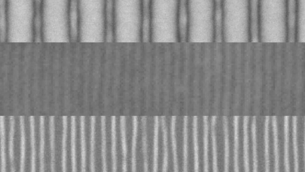
The research revolves around the self-assembly of wires on chips. The wires would handle the biggest challenge in chip making. Instead of etching fine features onto silicon using existing methods, materials called block copolymers would expand and self assemble into predefined designs and structures.
The implementation of such self-assembly technology will involve adding one step into existing chip manufacturing technologies, said Karen Gleason, a professor at the department of chemical engineering at MIT. Today’s manufacturing technology involves burning circuit patterns on to silicon wafers via masks using long wavelengths of light.
Chips are currently being manufactured at the 10nm process, and it’s becoming difficult to cram smaller transistors using the same wavelength. Extreme ultra-violet (EUV) lithography is expected to reduce wavelengths, helping etch finer features on to chips. EUV is expected to come online with the manufacturing of 7nm chips. But even though billions of dollars have been invested to implement EUV, it still remains a challenge to deploy.
MIT meanwhile claims its technology can easily slip into existing manufacturing technologies without additional complications. Using standard lithography technologies, block copolymer material can be deposited on a predetermined surface pattern to create wires. The block copolymers have two different polymers that are connected like a chain.
After that, a protective polymer layer is placed on the block copolymer through a process called chemical vapor deposition. That causes the block copolymers to self-assemble into vertical layers. This is similar to how 3D transistors are constructed today. The technology can be used to create complex self-assembling patters and layers. The technology can be applied to the 7nm manufacturing process.
IDG News Service


Subscribers 0
Fans 0
Followers 0
Followers